controls are our passion

PCB assembly
PCB assembly

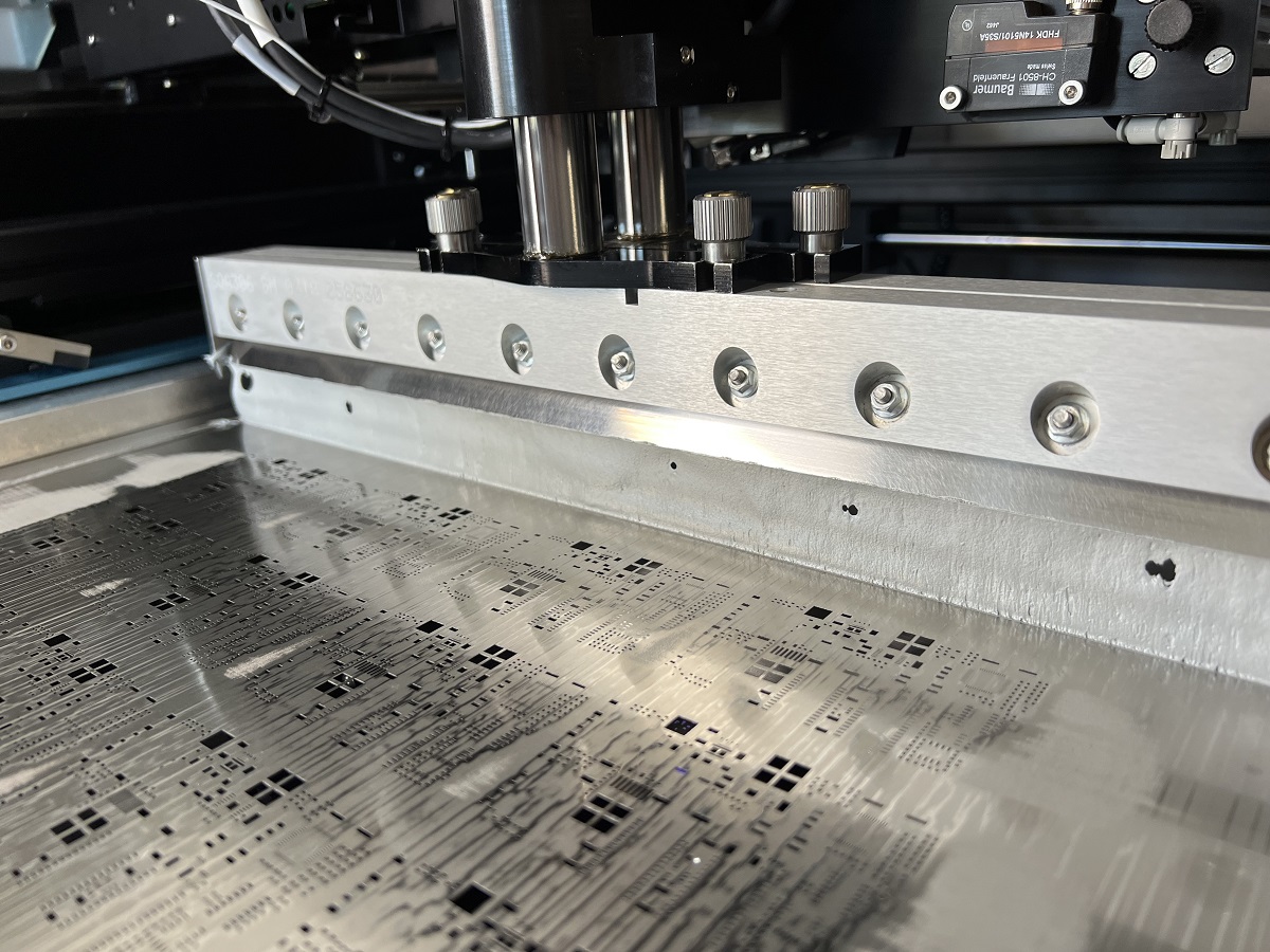
In principle, there are two different processes – SMD assembly and THT assembly.

SMD assembly (Surface Mounted Device)

When assembling the SMD, components are soldered straight onto a circuit board using solderable terminal surfaces. This may result in very high component density and assembly on both sides, which can have a positive effect on the electrical properties. This means that less assembly space is required, which also means that devices can be made smaller and produced in a more cost-effective way.

We have two assembly lines consisting of three SMD placement machines and one automatic soldering paste printer. The soldering process takes place in our convection reflow soldering machine.

THT assembly (Througth Hole Technology)

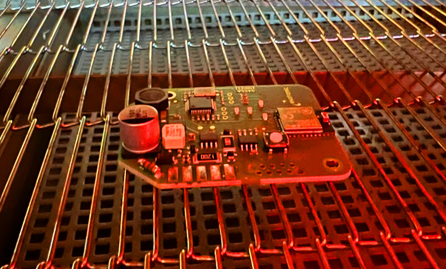
In contrast to SMD assembly, THT assembly is characterised by the fact that the components have wire connections. During assembly, they are inserted into so-called contact holes through a circuit board and must be soldered afterwards. Although THT assembly has dwindled as part of the miniaturisation of components in recent years, there are components (connectors, contact strips and the like) that are still designed as THT parts.

THT assembly is carried out manually. In addition to conventional manual soldering, we also use wave soldering machines that are more economical for a larger number of solder joints and guarantee consistent quality.


Soldering paste printing

As the first step in the production process, soldering paste is applied to blank circuit boards during soldering paste printing. For this purpose, a product-specific template is clamped into the soldering paste printer, which is recessed in the places where the soldering paste is to be printed on the circuit board. Absolute precision is required for this process. A lack of soldering paste or solder straps are frequently the cause of breakdowns in production and in the field.

Our system carries out checks with a camera after every application process to ensure error-free printing and automatically cleans the template after the process has been carried out a set number of times.

Placement machine

SMD assembly takes place in the second step. An application head with multiple sockets takes in the electronic components to be placed from so-called feeders, then uses a camera to measure the position of the component on the dropper and positions it by monitoring the pressure on the corresponding pad on the circuit board. Our new placement machine from Siplace wins points here thanks to its high levels of precision and performance. Components with a construction form up to 01005 can be processed.

Reflow

Components that are only stuck down with adhesive must be soldered to the circuit board later. For this purpose, the circuit board goes through a reflow oven with different temperature zones. With a brief peak temperature of 260°C, the soldering paste melts and ensures the component has a firm connection to the terminal surface in the subsequent cooling process. The components will then be firmly bonded to the circuit board.

Solder joint inspection

The defined solder joints will then be inspected on a random basis. For this purpose, we use a 3D coordinate measuring system from Keyence. The precise way in which the solder joints must be created is regulated in IPC-A-610E (Acceptability of Electronic Assemblies).

2023 © Exotronic GmbH Data protection Imprint